Range of AnalysesCompositional Analysis

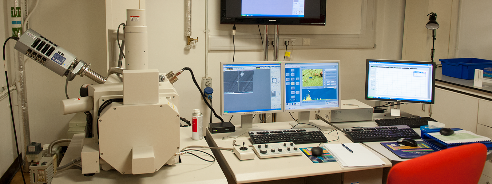
Scanning Electron Microscopes (SEM)
- Two SEMs - a Field Emission SEM (HITACHI SU-6600) and a Tungsten Filament SEM (HITACHI S-3700)
- A five-segment backscattered electron (BSE) detector for material composition imaging
- Elemental analysis and mapping by energy dispersive spectroscopy (EDS)
- Wavelength dispersive spectroscopy (WDS) for concentrations ≤500ppm or element overlaps (e.g. Mo/S)
- Scanning transmission electron microscopy (STEM) on thin films
- Variable pressure mode for non-conductive specimens – i.e. no need for carbon/gold coat
- Non-destructive analysis on small components through a large chamber (300 x 110mm)
- In-situ micro-mechanical tests (2kN load cell & video capture)
- Environmental capability.

Glow Discharge - Optical Emission Spectrometer (GD-OES)
- The only GD-OES in Scotland and one of four in UK
- For qualitative and quantitative elemental analysis, and depth profiling (up to 150μm) of conducting and non-conducting materials
- Measures simultaneously multiple elements present in the material analysed
- High sensitivity to all elements (including gaseous or carbon)
- Provides elemental information for thin layers and coated components with a resolution of 1nm, where chemistry at the coating-substrate interface becomes paramount.

X-Ray Diffractometer (XRD)
- The BRUKER D8 ADVANCE with DAVINCI XRD extracts structural information material and phase identification from metals and ceramics
- Analysis can be completed at ambient and elevated temperatures up to 2000oC
- Specimens can be in bulk or powder form, thin films, corrosion products or debris
- Measured properties include phase composition, crystal structure, lattice parameters and mismatches, spatial orientation of crystals, crystallinity, residual stress, grain texture, and layer thickness.

Example of a profile the GD-OES can produce